Ultra-Low Resistance Shunts Below 0.1 mΩ: Design Challenges in High-Current Sensing
Reducing shunt resistance is an effective way to limit insertion loss in high-current systems. But once the resistance falls below 0.1 mΩ, the design problem changes significantly. The resistor may dissipate less power, yet the voltage available for measurement also becomes smaller, leaving less margin for amplifier offset, ADC resolution, thermal effects, and parasitic resistance.
This trade-off is easy to overlook because ultra-low resistance initially appears to solve the main weakness of resistive current sensing: power loss. In reality, a lower resistance transfers part of the design burden from the power path to the measurement chain.
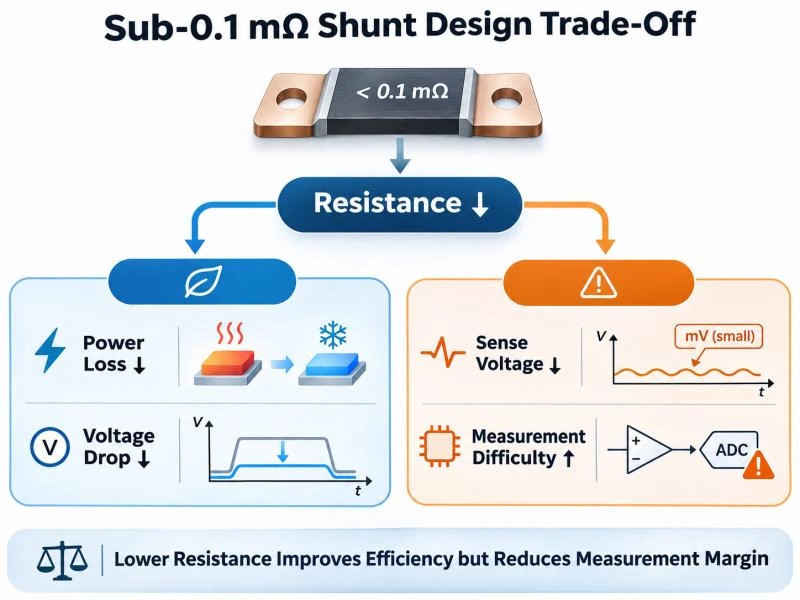
At 100 A, for example, the difference is already clear:
| Shunt Resistance | Sense Voltage at 100 A | Power Dissipation at 100 A |
|---|---|---|
| 0.10 mΩ | 10 mV | 1.00 W |
| 0.05 mΩ | 5 mV | 0.50 W |
| 0.025 mΩ | 2.5 mV | 0.25 W |
The power loss is reduced in direct proportion to resistance, which is beneficial. At the same time, however, the useful measurement signal is reduced by the same proportion.
The engineering question therefore changes from:
How low can the shunt resistance be made?
to:
How low can the resistance be while the complete sensing system can still resolve the current accurately and repeatably?
What Changes When Shunt Resistance Falls Below 0.1 mΩ?
There is no universal physical boundary at exactly 0.1 mΩ. The significance of this range comes from the relative size of the wanted signal compared with the unwanted electrical effects surrounding it.
At conventional milliohm values, a few micro-ohms of connection resistance or a few microvolts of amplifier offset may represent a relatively small fraction of the signal. At 0.05 mΩ or 0.025 mΩ, the same absolute error can consume a much larger part of the available measurement margin.
| Design Factor | As Shunt Resistance Decreases | Engineering Consequence |
|---|---|---|
| Sense Voltage | Decreases | Greater demand on amplifier and ADC resolution |
| Insertion Loss | Decreases | Improved efficiency in high-current paths |
| Self-Heating at the Same Current | Decreases | More thermal margin, assuming identical conditions |
| Relative Influence of Parasitic Resistance | Increases | Terminal, busbar and interconnect design become more critical |
| Relative Influence of Offset and Thermal EMF | Increases | Microvolt-level errors become more important |
This is why a sub-0.1 mΩ shunt should not be treated as simply a lower-value version of a conventional current sense resistor. The resistor, terminals, current path, sense amplifier, ADC, and thermal environment increasingly behave as one measurement system.
The First Challenge Is Signal Amplitude
A shunt produces a voltage proportional to current:
Vsense = I × Rshunt
When the resistance is extremely small, this voltage can remain in the millivolt range even at substantial current.
Consider a 0.025 mΩ shunt. At 100 A, the output is only 2.5 mV. At 20 A, it falls to 0.5 mV. A sensing circuit that must accurately measure both high load and low load therefore has to resolve signals spanning a very small absolute voltage range.
Low-Current Accuracy Becomes More Difficult
The highest current in the system is not always the hardest point to measure. At high current, the shunt produces a larger voltage signal. At light load, the signal becomes smaller while several error sources remain relatively unchanged.
For example, amplifier input offset does not fall simply because the current is lower. ADC quantization, reference error, switching noise, and thermoelectric offsets can therefore occupy a larger percentage of the measured signal at low current.
Ultra-low resistance improves the power path, but it reduces the electrical margin available to the measurement path.
ADC Resolution Has to Be Evaluated at the Minimum Useful Current
ADC resolution should not be checked only at full-scale current. The more important question is whether the smallest current that matters to the control system still produces enough measurable voltage above noise and offset.
Suppose a design uses a 0.05 mΩ shunt:
| Current | Ideal Shunt Voltage |
|---|---|
| 300 A | 15 mV |
| 100 A | 5 mV |
| 20 A | 1 mV |
| 5 A | 0.25 mV |
The 300 A measurement may be relatively straightforward, while the 5 A condition demands much more from the amplifier and converter. This is why the useful current range—not only the maximum current—should define the measurement architecture.
Lower Resistance Reduces Power Loss, but Not Without Trade-Offs
The main reason to use an ultra-low resistance shunt is often efficiency. The resistor is placed directly in the power path, so any voltage drop across it represents real energy loss.
The dissipation is:
P = I²R
At a fixed current, halving the resistance halves the shunt dissipation. This becomes valuable when current reaches hundreds of amperes.
For a 0.1 mΩ shunt:
| Current | Sense Voltage | Ideal Dissipation |
|---|---|---|
| 100 A | 10 mV | 1 W |
| 200 A | 20 mV | 4 W |
| 300 A | 30 mV | 9 W |
The quadratic relationship with current is important. Even an extremely small resistance can generate meaningful heat once current becomes sufficiently high.
Ultra-Low Resistance Does Not Eliminate Thermal Design
It is therefore incorrect to assume that a sub-0.1 mΩ shunt has negligible thermal requirements. The actual operating temperature still depends on continuous current, package construction, terminal design, ambient temperature, heat spreading, mounting structure, and the manufacturer's derating conditions.
Prosemi's current 2nd-Generation Custom Shunt Resistor range illustrates the type of power level involved in these applications: the PHS series covers 0.025–0.1 mΩ with power ratings from 25 W to 50 W. These ratings reflect use in genuinely high-current sensing paths rather than low-power signal circuits.
The design objective is therefore not simply to minimize resistance. It is to balance two competing requirements:
Low enough resistance to control loss and temperature rise, but high enough signal voltage for the measurement chain to maintain the required accuracy.
Parasitic Resistance Becomes a Larger Percentage of the Measurement
As shunt resistance moves into the tens of micro-ohms, parasitic resistance stops being a small background effect and can become a meaningful fraction of the measured value.
Consider a 0.05 mΩ shunt:
0.05 mΩ = 50 μΩ
If the surrounding current path contributes only 5 μΩ of additional effective resistance, that extra resistance is already equivalent to 10% of the nominal shunt value.
At 0.025 mΩ, the same 5 μΩ contribution would represent 20%.
| Nominal Shunt Resistance | Additional Parasitic Resistance | Parasitic Resistance as % of Shunt |
|---|---|---|
| 0.10 mΩ | 5 μΩ | 5% |
| 0.05 mΩ | 5 μΩ | 10% |
| 0.025 mΩ | 5 μΩ | 20% |
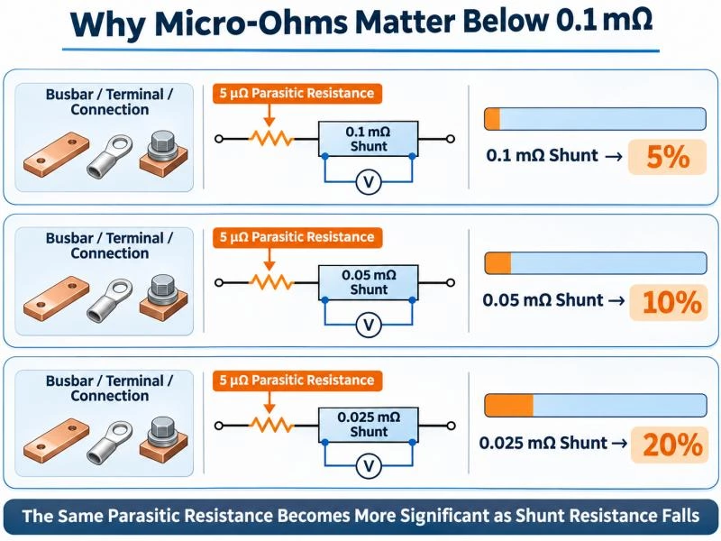
This is the reason sub-0.1 mΩ sensing becomes highly sensitive to the electrical structure around the resistor. A few micro-ohms that would be insignificant in a higher-resistance component can become large enough to distort the current calculation.
The Shunt Element Is No Longer the Only Relevant Resistance
The real current path can include several small resistive contributions:
- shunt alloy element,
- copper terminals,
- busbar interfaces,
- welded joints,
- PCB copper,
- mechanical connections.
At ultra-low resistance values, these elements should not automatically be treated as electrically negligible.
The measurement architecture therefore has to distinguish between:
the resistance intentionally used for current sensing
and:
the resistance that exists only because current must physically enter and leave the component.
Below 0.1 mΩ, micro-ohms matter.
The lower the shunt resistance becomes, the more carefully terminal, interconnect and current-path contributions must be controlled.
Why Copper Terminals Matter More at Ultra-Low Resistance
A high-current shunt is not made only from resistive alloy. The current also passes through conductive terminals, which are often designed to minimize resistance while providing a robust electrical and mechanical connection.
At conventional resistance values, the terminal contribution may represent a relatively small part of the total measured resistance. At 0.1 mΩ and below, it can become much more significant.
This is especially important because the temperature behavior of the terminal material may differ from that of the resistive alloy.
Alloy TCR Does Not Describe the Complete Installed Device
Temperature coefficient of resistance, or TCR, describes how resistance changes as temperature changes. It is often used as a key indicator of current-sensing stability.
However, in an ultra-low resistance design, the TCR of the resistive alloy alone may not fully describe the behavior of the complete current path.
A useful example comes from a 0.1 mΩ current-sense resistor family referenced in the industry literature. The resistive alloy is specified at ±50 ppm/°C, while the value including copper terminals is specified at ±275 ppm/°C over the stated temperature range.
The exact values are product-specific, but the engineering lesson is broader:
When the nominal resistance is extremely low, the temperature behavior of terminals and interconnects can become a significant part of the total resistance change.
Copper Resistance Changes with Temperature
Copper has a positive temperature coefficient. As terminal, busbar, or PCB copper temperature rises, its resistance increases.
If the voltage-sense points include part of this copper path, the measured voltage can change even when the alloy element itself remains relatively stable.
This creates a system-level temperature dependency that may not be visible from the nominal resistance tolerance alone.
Thermal Gradients Matter More Than Uniform Temperature Rise
A current shunt rarely operates at one perfectly uniform temperature. The resistive element, copper terminals, busbar, PCB copper, and nearby power components can all reach different temperatures.
This creates a thermal gradient across the sensing structure.
For example:
- one terminal may be closer to a hot MOSFET or busbar,
- one side may have more copper for heat spreading,
- airflow may cool one end more effectively than the other,
- current density may not be perfectly symmetrical.
These differences matter because resistance and thermoelectric effects depend on local temperature, not only on average ambient temperature.
Symmetrical Thermal Design Helps Preserve Measurement Stability
In high-accuracy ultra-low resistance sensing, electrical symmetry and thermal symmetry should be considered together.
Useful design principles include:
- keeping both terminals in similar thermal environments,
- avoiding strong local heat sources near only one side of the shunt,
- using balanced copper geometry where practical,
- routing sense connections from equivalent positions on both sides.
The objective is not to eliminate temperature rise completely, but to reduce uncontrolled temperature differences across the measurement structure.
Thermal EMF Becomes Relevant When the Sense Signal Is Only a Few Millivolts
Thermal electromotive force is another effect that becomes more important as the useful shunt signal becomes smaller.
When dissimilar conductive materials are joined and a temperature difference exists between the junctions, a small thermoelectric voltage can be generated.
In many power circuits this voltage is negligible. In a sub-0.1 mΩ shunt producing only a few millivolts—or less at low current—the same microvolt-level offset can become a meaningful fraction of the measured signal.
Why Thermal EMF Matters More at Low Current
Suppose a 0.025 mΩ shunt is measuring 20 A:
Vsense = 20 A × 0.025 mΩ = 0.5 mV
At that operating point, the signal is only 500 μV.
A small thermoelectric offset that would be insignificant compared with a 50 mV signal becomes much more important relative to 500 μV.
This is why low thermal EMF becomes a useful characteristic in ultra-low resistance shunt designs, especially when the measurement range includes relatively low current as well as very high current.
Thermal EMF and TCR Are Different Error Mechanisms
These two effects should not be confused.
| Effect | What Changes | Measurement Consequence |
|---|---|---|
| TCR | Electrical resistance changes with temperature | The current-to-voltage conversion ratio changes |
| Thermal EMF | A thermoelectric voltage is generated by material junctions and temperature differences | An additional offset voltage can appear in the sensed signal |
Both become more important as the nominal shunt signal becomes smaller, but they enter the error budget in different ways.
Ultra-Low Resistance Requires a System-Level Error Budget
At 0.1 mΩ and below, no single specification fully describes current-measurement accuracy.
A realistic error budget may need to include:
- shunt resistance tolerance,
- alloy TCR,
- terminal and copper temperature effects,
- parasitic resistance,
- thermal EMF,
- amplifier offset and gain error,
- ADC resolution and reference error.
The design challenge is therefore not simply to find the lowest possible resistance value. It is to ensure that the complete measurement system can still separate the true current signal from the electrical and thermal effects surrounding it.
Low Inductance Matters in Fast Current Transients
For steady DC current, the voltage across a shunt is usually described by the familiar relationship V = IR. In fast-switching power systems, however, the shunt is not perfectly resistive. Its physical structure, terminals, and current path introduce a small amount of parasitic inductance.
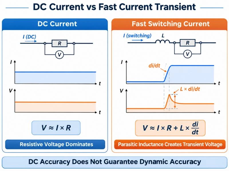
When current changes rapidly, the measured voltage can therefore contain both a resistive component and a transient inductive component:
Vmeasured ≈ I × R + L × di/dt
For a conventional current measurement with a relatively slow current waveform, the inductive term may be small enough to ignore. In an inverter, motor drive, DC/DC converter, or other high-speed switching system, the rate of current change can be large enough for even a few nanohenries of inductance to influence the waveform.
The lower the shunt resistance becomes, the more important parasitic inductance can become relative to the intended resistive voltage.
Why the Effect Becomes More Visible Below 0.1 mΩ
Consider two shunts carrying the same rapidly changing current. If one shunt has a resistance of 1 mΩ and the other only 0.05 mΩ, the second device produces just one-twentieth of the resistive voltage for the same current.
The parasitic inductance does not necessarily decrease by the same factor.
As a result, the ratio between the unwanted L × di/dt voltage and the desired I × R voltage can increase significantly.
This is one reason ultra-low resistance current sensing resistors intended for fast-switching power systems require careful structural design rather than simply a low nominal resistance value.
Fast Switching Can Distort the Apparent Current Waveform
Suppose a power stage experiences a current transition of 200 A within 1 μs. The rate of change is:
di/dt = 200 A/μs
With only 2 nH of parasitic inductance, the transient inductive voltage would be approximately:
V = L × di/dt = 0.4 V
That transient is much larger than the millivolt-level resistive voltage produced by a sub-0.1 mΩ shunt.
This does not mean the current measurement will continuously show a 0.4 V error. The inductive voltage is associated with the rapid transition itself. However, it demonstrates why switching edges, ringing, amplifier bandwidth, filtering, and sense-path geometry become important when measuring dynamic current.
DC Accuracy and Dynamic Accuracy Are Not the Same
A shunt can produce excellent results in a DC resistance test and still show very different behavior when used to capture high-frequency current transients.
DC accuracy is dominated by factors such as resistance tolerance, TCR, amplifier offset, and thermal conditions. Dynamic accuracy adds another group of variables:
| DC Measurement | Dynamic Current Measurement |
|---|---|
| Resistance tolerance | Resistance tolerance |
| TCR | TCR |
| Amplifier offset | Amplifier bandwidth |
| Thermal EMF | Parasitic inductance |
| ADC resolution | Switching noise and ringing |
| Steady-state layout effects | High-frequency sense-loop geometry |
This distinction is particularly important when a shunt is part of a control loop rather than only a protection or monitoring function.
In a motor inverter, for example, the controller may need current information quickly enough to regulate phase current or detect an abnormal event. A current-sensing path with excellent low-frequency accuracy but poor transient behavior may not provide the information required at the correct moment.
Low Inductance Is a System Requirement, Not Just a Resistor Specification
Selecting a low-inductance shunt helps, but the complete current path still matters.
Large loops formed by the shunt, busbar, sense conductors, and amplifier input can introduce additional inductive pickup. The measurement should therefore be considered as a combination of:
shunt structure + high-current connection + sense routing + amplifier bandwidth + filtering.
The resistor alone cannot compensate for a poorly designed measurement loop.
Continuous Current and Pulse Overload Must Be Evaluated Separately
Ultra-low resistance shunts are often selected for systems carrying hundreds of amperes, where the current is not always constant. Motor startup, inverter transients, capacitor charging, short-duration acceleration, and fault events can all create current peaks substantially above the normal operating level.
This makes it important to distinguish between continuous power handling and short-duration overload capability.
Continuous Current Is Primarily a Thermal Problem
Under steady current, the shunt continuously converts electrical energy into heat according to:
P = I²R
The resulting temperature depends on more than the rated wattage printed in a product table. Heat must move from the resistive element through the terminals and into the PCB, busbar, enclosure, or surrounding air.
A useful continuous-current evaluation therefore considers:
- maximum RMS current,
- ambient operating temperature,
- available copper or busbar area,
- thermal resistance of the installation,
- allowed temperature rise,
- manufacturer derating requirements.
High-current metal alloy shunt resistors are designed to handle demanding power paths, but the final usable current still depends on the complete thermal environment.
Pulse Current Is an Energy and Time Problem
A short pulse can exceed the nominal continuous current without immediately driving the entire resistor to its steady-state temperature. The component has thermal mass, so a brief event may deposit energy faster than that energy can spread through the structure.
However, this does not mean any short pulse is acceptable.
Pulse capability depends on several variables at the same time:
| Parameter | Why It Matters |
|---|---|
| Peak Current | Determines instantaneous I²R stress |
| Pulse Duration | Controls how much energy is deposited |
| Duty Cycle | Determines whether heat can dissipate between pulses |
| Initial Temperature | Changes the available thermal margin |
| Mechanical Construction | Influences local current density and thermal stress |
For this reason, a 50 W shunt should not automatically be assumed to tolerate a specific overload simply because the average calculated power remains below 50 W.
Repeated pulses can also create a very different thermal condition from one isolated pulse.
High Overload Capability Does Not Replace Pulse Validation
Prosemi's 2nd-generation custom shunt resistors are designed for ultra-low resistance, high-current applications and emphasize high overload capability. That characteristic is useful in systems where operating current is not perfectly steady.
But overload capability should still be evaluated against the actual current profile of the application rather than treated as a generic multiplier of continuous power.
For example, these three operating conditions may have the same peak current but impose very different stress:
500 A for 100 μs
500 A for 20 ms
500 A repeated every 100 ms
The electrical peak is identical, but the energy deposited and the resulting temperature rise are not.
Busbar and Terminal Design Become Part of the Sensing System
When current reaches hundreds of amperes, the shunt is rarely an isolated component connected by narrow PCB traces. The surrounding power path may include heavy copper, busbars, welded terminals, mechanical fasteners, or custom conductors.
At that point, the physical connection becomes part of both the power design and the measurement design.
Current Distribution Should Be as Uniform as Practical
If current enters one side of the terminal unevenly, current density through the resistive element may become nonuniform. This can create localized heating and alter the voltage distribution around the sense points.
A symmetrical current path is therefore preferable where the mechanical design allows it.
The goal is not merely to carry the required current. It is to make the current distribution through the calibrated sensing region predictable.
Sense Points Should Exclude the High-Current Connection Drop
The voltage used for current calculation should represent the intended resistive element rather than uncontrolled voltage drop in the busbar, terminal, weld, or mechanical connection.
Kelvin sensing is commonly used to separate the measurement path from the force-current path. In a sub-0.1 mΩ design, this becomes particularly valuable because even a small additional voltage drop can represent a large percentage of the intended shunt signal.
However, Kelvin sensing is not a substitute for correct placement. If the voltage taps are positioned where substantial terminal or busbar resistance is already included, the circuit can still measure more than the calibrated shunt resistance.
Mechanical Symmetry Can Support Electrical Accuracy
Mechanical design is sometimes treated as separate from measurement accuracy, but the two are closely linked in ultra-high-current sensing.
Terminal geometry affects:
- current distribution,
- contact resistance,
- heat spreading,
- temperature gradients,
- parasitic inductance.
An asymmetric busbar structure can therefore introduce both electrical and thermal asymmetry even when the shunt resistor itself has excellent nominal specifications.
For custom high-current designs, the resistance value, current path, terminal geometry, mounting method, and sensing points should ideally be considered together rather than sequentially.
Where Sub-0.1 mΩ Shunts Make Engineering Sense
An ultra-low resistance shunt is not automatically the best choice for every current measurement. Its main advantage appears when current is high enough that conventional milliohm-level resistance would create excessive voltage drop, power loss, or temperature rise.
The strongest use cases are therefore applications where electrical efficiency and high-current capability justify the additional measurement complexity.
Very High Continuous Current
As continuous current rises, even a small resistance can dissipate substantial power because power increases with the square of current.
For example, at 300 A:
| Shunt Resistance | Voltage Drop | Power Dissipation |
|---|---|---|
| 1 mΩ | 300 mV | 90 W |
| 0.1 mΩ | 30 mV | 9 W |
| 0.05 mΩ | 15 mV | 4.5 W |
| 0.025 mΩ | 7.5 mV | 2.25 W |
This is where sub-0.1 mΩ resistance becomes attractive. The reduction in insertion loss can be significant enough to justify a more demanding amplifier, ADC, thermal, and layout design.
High-Efficiency Power Conversion
In converters and inverters, every additional millivolt of voltage drop contributes to conduction loss. A low-value shunt can reduce this burden while still providing a direct electrical measurement of current.
Typical examples include:
- high-power DC/DC converters,
- motor drives,
- industrial inverters,
- high-current power modules,
- power distribution stages.
In these applications, the required resistance value should be evaluated together with switching speed, measurement bandwidth, acceptable power loss, and the minimum current that still needs to be measured accurately.
Systems with Tight Power-Loss Budgets
A current sensor may be electrically accurate but still be unsuitable if it introduces too much energy loss into the power path.
This becomes particularly important in systems operating continuously at high current, where even a few watts of unnecessary loss can affect efficiency, enclosure temperature, cooling requirements, and long-term reliability.
For these applications, ultra-low resistance current sensing resistors can provide a practical balance between measurable voltage and reduced insertion loss.
When Going Below 0.1 mΩ May Not Be the Best Choice
Lower resistance should not be treated as an automatic improvement.
A shunt value that minimizes power loss but produces a signal too small for the sensing electronics can make overall current accuracy worse rather than better.
When the Current Is Too Low
If the normal operating current is modest, a 0.025 mΩ or 0.05 mΩ shunt may generate only a few hundred microvolts.
For example:
10 A × 0.025 mΩ = 0.25 mV
At this level, amplifier offset, noise, ADC resolution, thermal EMF, and reference accuracy may consume a large fraction of the useful signal.
In such a design, increasing the shunt resistance slightly may improve total system accuracy without creating unacceptable power loss.
When the Measurement Electronics Cannot Resolve the Signal
The minimum resistance should be chosen together with the measurement chain.
Before selecting an ultra-low resistance shunt, the designer should confirm that the amplifier and ADC can resolve the required current range with adequate margin.
A useful rule is:
Select the lowest resistance that still produces a reliably measurable signal across the required operating range—not simply the lowest resistance available.
When Parasitic and Thermal Errors Cannot Be Controlled
Reducing resistance can also make the system more sensitive to effects that are difficult to compensate later.
If the mechanical structure forces asymmetric current flow, the terminals experience large temperature differences, or the sense points cannot be positioned correctly, moving to a lower resistance may increase uncertainty.
In that situation, a slightly higher resistance with a cleaner and more stable measurement structure may provide better real-world performance.
Practical Design Checklist for Sub-0.1 mΩ Current Sensing
Before finalizing a sub-milliohm shunt design, the resistor should be evaluated as part of the complete sensing and power path rather than as an isolated component.
| Design Check | Engineering Question |
|---|---|
| Sense Voltage | Does the minimum useful current still generate enough voltage to measure reliably? |
| Full-Scale Voltage | Does maximum current remain within the amplifier and ADC input range? |
| Amplifier Offset | Is input offset small relative to the minimum shunt signal? |
| ADC Resolution | Are enough effective counts available at low current? |
| Continuous Power | Is I²R dissipation acceptable at maximum RMS current? |
| Thermal Path | Can heat move effectively into the busbar, PCB, or surrounding structure? |
| Parasitic Resistance | Are terminal and interconnect contributions small relative to the shunt value? |
| Thermal EMF | Could microvolt-level thermoelectric offsets affect low-current accuracy? |
| Parasitic Inductance | Will fast current transients introduce significant L × di/dt voltage? |
| Pulse Capability | Has peak current been checked against pulse duration and repetition rate? |
| Current Distribution | Does the busbar or terminal geometry drive current uniformly through the sensing element? |
| Sense-Point Placement | Do the voltage taps measure the intended resistive element rather than connection drop? |
Prosemi Ultra-Low Resistance Shunt Solutions
For applications requiring very low insertion loss at high current, Prosemi offers 2nd-generation custom shunt resistors with resistance values from 0.025 mΩ to 0.1 mΩ and power ratings from 25 W to 50 W.
The PHS series is designed around the requirements discussed throughout this article, including:
- ultra-low resistance for reduced conduction loss,
- low TCR for improved temperature stability,
- low thermal EMF for small-signal current measurement,
- high overload capability for demanding current profiles,
- customizable structures for high-current applications.
For applications that do not require resistance below 0.1 mΩ, Prosemi also provides a broader range of metal alloy shunt resistors and other current sensing resistor structures for different power, accuracy, package, and mounting requirements.
The correct resistance value should ultimately be selected from the complete system requirements rather than from resistance alone.
Conclusion
Moving below 0.1 mΩ changes the nature of current sensing.
The lower resistance can significantly reduce voltage drop and I²R loss in high-current power paths, but the useful sense voltage also becomes smaller. As a result, amplifier offset, ADC resolution, parasitic resistance, terminal behavior, thermal gradients, thermal EMF, and parasitic inductance all take on greater importance.
The design relationship can be summarized simply:
Lower Resistance → Lower Power Loss → Lower Sense Voltage → Greater Measurement Demands
For high-current systems, an ultra-low resistance shunt can provide an effective combination of efficiency and direct current measurement. The key is to treat the resistor, current path, sensing electronics, and thermal structure as one measurement system.
If your application requires resistance in the 0.025–0.1 mΩ range, contact Prosemi to discuss current level, power requirements, resistance value, mechanical structure, and customization options.
FAQ
Why use a shunt resistor below 0.1 mΩ?
The main reason is to reduce voltage drop and power loss in very high-current circuits. At hundreds of amperes, even a fraction of a milliohm can dissipate significant power, so reducing resistance can improve efficiency and thermal performance.
How much voltage does a 0.1 mΩ shunt produce at 100 A?
Using V = IR, a 0.1 mΩ shunt carrying 100 A produces 10 mV. At 200 A it produces 20 mV, and at 300 A it produces 30 mV.
Is a lower shunt resistance always better?
No. Lower resistance reduces insertion loss, but it also reduces the measurement signal. If the signal becomes too small relative to amplifier offset, noise, ADC resolution, thermal EMF, or parasitic resistance, total measurement accuracy can deteriorate.
Why are sub-0.1 mΩ shunts harder to measure accurately?
Their output voltage is typically only a few millivolts or less. Because the useful signal is small, microvolt-level offsets and micro-ohm-level parasitic resistance represent a larger percentage of the measurement.
How does terminal resistance affect an ultra-low resistance shunt?
At resistance values such as 0.025 mΩ or 0.05 mΩ, even a few micro-ohms of terminal or interconnect resistance can represent a meaningful fraction of the nominal shunt resistance. Sense-point placement and current-path design therefore become critical.
Why does low inductance matter in high-current shunts?
In fast-switching systems, parasitic inductance produces an additional voltage proportional to L × di/dt. During rapid current transitions, this transient voltage can become much larger than the intended millivolt-level resistive signal.
What is thermal EMF in a shunt resistor?
Thermal EMF is a small thermoelectric voltage generated when dissimilar conductive materials experience a temperature difference. It becomes more important when the shunt signal itself is only hundreds of microvolts or a few millivolts.
When should a 0.025 mΩ shunt be considered?
A 0.025 mΩ shunt can be considered when current is sufficiently high that minimizing insertion loss is important and the sensing electronics can still resolve the resulting low voltage accurately. Thermal design, amplifier offset, ADC resolution, transient behavior, and connection resistance should all be evaluated before selecting such a low resistance.