How Parasitic Inductance Affects Current Sense Resistor Accuracy in High-Speed BMS Systems
TL;DR — If you only read one section:
Your shunt resistor's datasheet says 1% tolerance. Your actual current measurement error under switching conditions? Often 10–20% or more. The culprit isn't the resistor—it's parasitic inductance. In EV BMS systems, the real equation during transients is V = I × R + L × di/dt. That second term can saturate your ADC, false-trip your protection, and corrupt your SOC, all while your resistor is perfectly within spec.
I've debugged more "failed" current sense designs than I can count. And here's what I keep finding: the resistor is fine. The ADC is fine. The amplifier is fine. Everything measures perfectly with DC current. Then you put it in a real EV with real switching—and suddenly the readings go crazy.
The culprit? Almost always parasitic inductance. Not the resistor. Not the chip. The geometry.
The Equation That Changes Everything
In a textbook, current sensing is simple:
V = I × R
In an actual EV BMS during switching events, this is what your circuit actually sees:
V_sense = I × R + L × (di/dt)
That second term isn't a small correction. In high-speed systems, it often dominates the measurement entirely.
Here's what's happening: your shunt resistor isn't just a resistor. It's part of a current loop. That loop has inductance. When current changes rapidly—which it does constantly in an EV inverter—that inductance generates a voltage. That voltage appears right across your sense terminals. Your ADC can't tell the difference between "real current" and "inductive spike." It just sees voltage.
Where Parasitic Inductance Actually Comes From
Let's be specific. In a typical BMS shunt layout, parasitic inductance comes from four sources:
| Source | Typical Contribution |
|---|---|
| PCB trace loop area | 3–10 nH |
| Shunt resistor internal structure | 1–5 nH |
| Solder joint geometry | 0.5–2 nH |
| Power busbar connections | 2–8 nH |
Add them up. A well-optimized layout might hit 5–8 nH total. A typical production layout often measures 15–20 nH. A careless one? 30 nH or more.
And here's the trap: that inductance doesn't show up in your DC calibration. You can run a 10A DC test, see perfect linearity, and sign off on the design. Then the vehicle hits the road, the inverter starts switching, and your current readings become a mess. You spent weeks on that ADC selection. The ADC was never the problem.
di/dt: The Number Nobody Checks
In an EV, di/dt isn't a lab curiosity. It's a design parameter.
Typical numbers I've measured in production inverters:
- IGBT-based systems: 50–100 A/µs
- SiC-based systems: 100–200 A/µs (some exceed 250 A/µs)
Now run V = L × di/dt with realistic numbers:
| Parasitic Inductance | di/dt = 50 A/µs | di/dt = 100 A/µs | di/dt = 200 A/µs |
|---|---|---|---|
| 5 nH | 0.25 V | 0.5 V | 1.0 V |
| 10 nH | 0.5 V | 1.0 V | 2.0 V |
| 15 nH | 0.75 V | 1.5 V | 3.0 V |
| 20 nH | 1.0 V | 2.0 V | 4.0 V |
Let those numbers sit for a moment.
Most BMS ADC front ends run at 3.3V or 5V. At 15 nH and 100 A/µs, you're already at 1.5V of pure noise—before you measure a single amp of actual current. At 20 nH and 200 A/µs? That's 4.0V. You've saturated your ADC. The reading is meaningless.
And this is not a corner case. This is normal operation in a modern SiC-based EV traction system.
The False Trip Scenario: A Real Case
I worked on a BMS design where the protection circuit kept triggering during hard acceleration. The team swapped shunts. Adjusted ADC gain. Tweaked firmware filters. Nothing helped.
Here's what the root cause actually looked like:
- Shunt resistor: 1 mΩ, properly spec'd
- ADC: 3.3V full-scale, 16-bit
- PCB: production layout with about 15 nH loop inductance
- Inverter: SiC with ~120 A/µs switching
V_spike = 15 × 10−9 × 120 × 106 = 1.8V
That 1.8V spike appeared directly on the sense lines during every switching edge. The ADC saw it as current. The protection logic saw overcurrent. The system faulted.
The resistor was correct. The ADC was correct. The layout was not.
Why This Problem Is Getting Worse
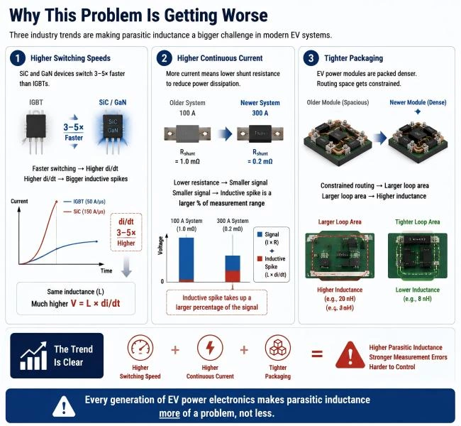
It's not your imagination. This issue is more severe today than five years ago:
1. Higher switching speeds. SiC and GaN devices switch 3–5× faster than IGBTs. Faster switching means higher di/dt. Higher di/dt means bigger inductive spikes for the same inductance.
2. Higher continuous current. More current means lower shunt resistance (to keep power dissipation down). Lower resistance means smaller signals. Smaller signals mean the inductive spike is a larger percentage of your measurement range.
3. Tighter packaging. EV power modules are packed denser. Denser packaging often means larger loop area because routing gets constrained. Larger loop area = higher inductance.
The trend is clear: every generation of EV power electronics makes parasitic inductance more of a problem, not less.
Why Two Identical Shunts Behave Differently
This is the part that confuses engineers. You buy the same shunt from the same reel. Populate two boards. One reads cleanly under switching. The other is noisy.
The difference is rarely the resistor. It's the geometry around it.
Small differences in layout matter:
| Layout Variable | Impact on Inductance |
|---|---|
| Sense trace separation | Wider spacing = larger loop = higher L |
| Sense trace length | Longer = higher L |
| Return path distance | Farther = higher L |
| Ground plane under sense lines | Solid plane reduces loop area = lower L |
I've seen identical BOMs produce 8 nH vs 18 nH parasitic inductance—just from routing differences on different PCB revision layers. Same components. Same schematic. Completely different transient behavior.
The Real-World Impact on BMS Accuracy
Parasitic inductance doesn't just cause noise. It has concrete system-level consequences:
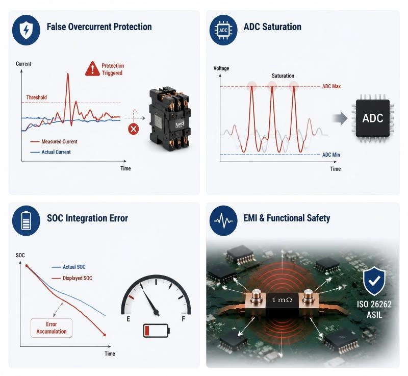
False overcurrent protection. This is the most common symptom. The protection trips. The contactor opens. The vehicle derates. Customer complains. Engineering team blames software. Software blames hardware. And the actual root cause is a 15 nH layout loop.
ADC saturation. When the spike exceeds the ADC input range, you lose that sample. The firmware discards it, or worse, averages it in. Either way, you lose measurement bandwidth. In safety-critical current monitoring, lost samples mean lost confidence.
SOC integration error. Coupled with TCR drift, inductive spikes add a time-varying offset to your current reading. The BMS integrates this error over time. Range estimation drifts. The vehicle shows 20% SOC and then dies at 15%. This is not hypothetical—I've seen it in field data.
EMI and functional safety. A high-energy spike on the sense lines isn't just an accuracy issue. It can inject noise into adjacent analog circuitry. It can affect comparator thresholds. It can violate ISO 26262 ASIL requirements if not properly characterized.
Engineering Solutions That Actually Work
Here's the practical playbook. Not theory. What I've actually used to fix these problems in production designs.
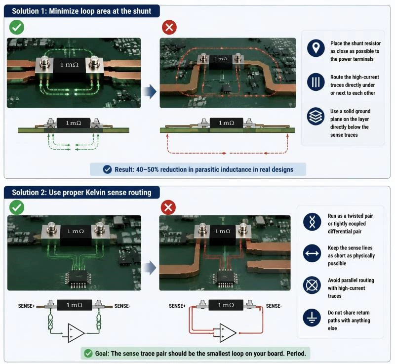
Solution 1: Minimize loop area at the shunt
The current loop needs to go out and back. The smaller the area between the outgoing and returning current path, the lower the inductance.
- Place the shunt resistor as close as possible to the power terminals
- Route the high-current traces directly under or next to each other
- Use a solid ground plane on the layer directly below the sense traces
I've seen this alone cut parasitic inductance by 40–50%.
Solution 2: Use proper Kelvin sense routing
This is critical. The Kelvin sense lines should:
- Run as a twisted pair or tightly coupled differential pair
- Stay as short as physically possible
- Avoid parallel routing with high-current traces
- Not share return paths with anything else
The sense trace pair should be the smallest loop on your board. Period.
Solution 3: Choose low-inductance shunt structures
Not all shunt resistors are created equal. Some internal structures are much lower inductance than others:
| Shunt Structure | Typical Inductance | Best For |
|---|---|---|
| Standard 2-terminal | 5–10 nH | Low-speed / DC applications |
| 4-terminal Kelvin | 3–8 nH | General BMS |
| Metal strip with reverse geometry | 1–3 nH | High-speed SiC / GaN systems |
| Coaxial / AEC-Q200 automotive | <2 nH | Safety-critical high-speed |
If you're designing for SiC, don't use a standard 2-terminal shunt. The inductance alone will defeat your measurement accuracy. Talk to your resistor supplier. Ask for low-inductance package options. They exist.
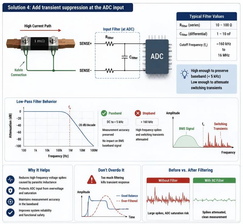
Solution 4: Add transient suppression at the ADC input
A small RC filter right at the ADC input can knock down high-frequency spikes without affecting your DC or low-frequency measurement bandwidth.
Typical values I've used:
- R_filter = 10–100 Ω (in series with the sense line)
- C_filter = 1–10 nF (differential between sense+ and sense-)
This forms a low-pass filter with cutoff frequency around 160 kHz to 16 MHz. High enough not to affect your baseband measurement (typically <5 kHz for BMS), low enough to attenuate switching transients.
But don't overdo it. Too much filtering kills your transient response. You need to balance measurement accuracy with transient protection. This is where simulation helps.
Solution 5: Validate with actual switching measurements
Here's the hard truth: DC testing is not enough. You need to measure with actual switching conditions.
I recommend this test protocol:
- Set up a current source with a realistic di/dt (use a MOSFET or IGBT pulsing circuit if you don't have an inverter)
- Measure the sense voltage with a differential probe
- Compare the waveform to your simulation
- Tweak layout until the measured inductance matches your target
Do this early. Before you commit to production layout. It's much cheaper to fix inductance on a prototype than on a shipping product.
A Simple Quick-Check Formula
Here's a back-of-the-envelope test you can run right now:
L_max = V_ADC_max / di/dt_max
- V_ADC_max = your ADC's usable input range (e.g., 3.0V out of 3.3V full-scale)
- di/dt_max = your worst-case switching speed (e.g., 150 A/µs)
For example:
L_max = 3.0V / 150 A/µs = 20 nH
That's your absolute maximum tolerable parasitic inductance. Anything above this, you'll see ADC saturation.
Now take your estimated loop inductance from your layout. If it's near or above this number, you have a problem. Fix it in layout, not in software.
Summary Table
| Factor | Impact | Mitigation |
|---|---|---|
| PCB loop area | Primary source of L | Route traces tight, use ground plane |
| Kelvin routing | Determines measurement integrity | Dedicated diff pair, short path |
| Shunt package | 1–10 nH variation | Choose low-inductance package for SiC |
| di/dt switching speed | Determines voltage spike amplitude | If >100 A/µs, layout is critical |
| ADC full-scale range | Defines L tolerance | Lower range → more L-sensitive |
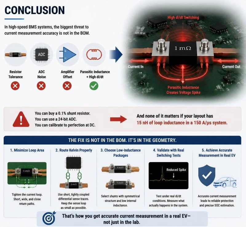
Conclusion
In high-speed BMS systems, the biggest threat to current measurement accuracy isn't resistor tolerance. It isn't ADC noise. It isn't amplifier offset.
It's parasitic inductance combined with high di/dt switching.
You can buy a 0.1% shunt resistor. You can use a 24-bit ADC. You can calibrate to perfection at DC. And none of it matters if your layout has 15 nH of loop inductance in a 150 A/µs system.
The fix is not in the BOM. It's in the geometry.
Minimize loop area. Route Kelvin properly. Choose low-inductance packages. Validate with real switching tests. That's how you get accurate current measurement in a real EV—not just in the lab.
FAQ
Q: Can't I just filter out the spikes in firmware?
Yes and no. Software filtering can hide the symptom, but it can't fix the root cause. You'll lose measurement bandwidth and transient response. In safety-critical systems, that's not acceptable.
Q: How much parasitic inductance is "too much"?
Use the formula above: L_max = V_ADC_max / di/dt_max. If your layout exceeds that, you'll see saturation.
Q: Does the shunt resistor's datasheet specify inductance?
Some do. Many don't. Ask your supplier. For high-speed applications, this spec is as important as resistance tolerance.
Q: Does Kelvin routing really help with inductance?
Absolutely. It separates the sense path from the current path. The sense loop area becomes tiny. That's exactly what you want.
Q: What's the difference between SiC and IGBT in this context?
SiC switches 2–3× faster. That means 2–3× higher di/dt for the same layout. So SiC systems are 2–3× more sensitive to parasitic inductance. You need to be much more careful with layout.
Q: Can I measure inductance on a finished PCB?
Yes. Use a network analyzer or an LCR meter with a proper test fixture. Or use a pulse current source and measure the transient response. The math is the same: V = L × di/dt, so measure di/dt and the resulting voltage spike, and solve for L.