SiC / GaN Inverter Current Sensing with Shunt Resistors
In modern power electronics, current sensing with shunt resistors has evolved from a straightforward electrical measurement into a multidisciplinary engineering challenge. This transformation is largely driven by the rapid adoption of silicon carbide (SiC) and gallium nitride (GaN) power devices in electric vehicles, renewable energy systems, industrial motor drives, and high-efficiency power converters.
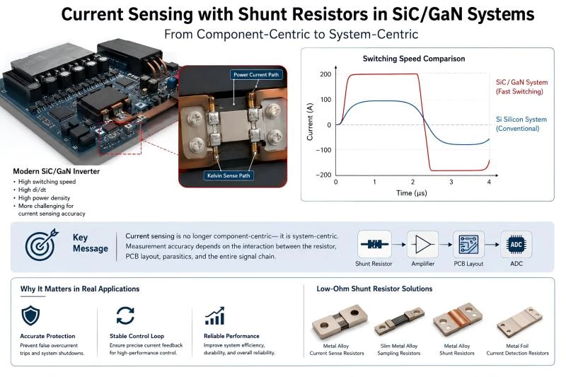
Unlike conventional silicon-based designs, today's inverter systems switch much faster and operate at significantly higher power densities. As a result, current sensing accuracy is influenced not only by resistor tolerance, but also by PCB layout, parasitic inductance, electromagnetic interference (EMI), thermal behavior, and signal conditioning.
For hardware engineers, choosing the correct current sensing resistor is therefore only one part of the design process. The resistor, measurement amplifier, PCB layout, Kelvin connection, and ADC all work together as a single measurement system.
A high-precision resistor cannot compensate for a poorly designed sensing loop. Likewise, an excellent PCB layout cannot fully overcome the limitations of an unsuitable shunt resistor. Reliable current measurement requires both.
Introduction: Why Current Sensing Changes in SiC / GaN Systems
SiC MOSFETs and GaN HEMTs have fundamentally changed the design philosophy of modern power electronics. Compared with traditional silicon IGBTs and MOSFETs, these wide-bandgap semiconductor devices switch faster, operate at higher temperatures, and significantly reduce switching losses. These advantages make them the preferred choice for next-generation EV traction inverters, fast chargers, photovoltaic inverters, and industrial power conversion systems.
However, higher efficiency comes with a new engineering challenge. As switching transitions become steeper, electrical parasitics that were previously insignificant begin to dominate the measurement circuit.
| Design Characteristic | Conventional Silicon Systems | SiC / GaN Systems |
|---|---|---|
| Switching Speed | Moderate | Extremely fast |
| Current Waveform | Relatively smooth | High transient content |
| Measurement Challenge | Resistor accuracy | System-level parasitics |
| Dominant Error Source | Tolerance & TCR | Layout, inductance and EMI |
In traditional converter designs, engineers mainly focused on selecting the correct resistance value, power rating and temperature coefficient. If these parameters met the design target, current measurement was usually predictable.
Modern SiC and GaN inverter systems behave very differently. Fast switching edges expose every parasitic element in the current path. PCB copper traces become part of the resistor network. Small loop inductances generate measurable voltage spikes. Ground impedance introduces additional offset, while switching noise couples directly into differential sensing lines.
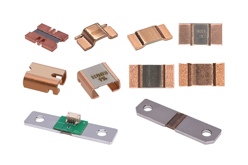
In other words, current sensing is no longer component-centric—it is system-centric. The measurement accuracy of a 0.5 mΩ shunt resistor is now determined as much by its installation environment as by its datasheet specifications. When selecting sensing components for these applications, engineers should evaluate not only resistance value but also package structure, pulse-current capability, and installation method. For high-current inverter designs, metal alloy shunt resistors are widely used because of their low resistance, excellent conductivity, and stable performance under heavy load conditions.
Many prototype failures attributed to "poor resistor accuracy" are eventually traced back to PCB layout, grounding strategy, or Kelvin routing. Improving resistor tolerance from 1% to 0.1% rarely solves a layout-induced measurement problem.
How High di/dt Impacts Current Sensing Accuracy
The most significant change introduced by SiC and GaN technology is the dramatic increase in current slew rate, commonly expressed as di/dt. While conventional silicon inverters often operate with relatively moderate switching edges, SiC and GaN devices routinely achieve current transition rates well above 100 A/µs, with some high-performance systems exceeding 300 A/µs.
Under these conditions, the familiar current sensing equation no longer tells the whole story.
Ideally, the voltage across a shunt resistor follows Ohm's law:
V = I × R
In reality, another voltage component appears whenever current changes rapidly:
V = I × R + L × di/dt
The second term is generated by parasitic inductance in the resistor package, PCB traces, busbars, solder joints and current loop geometry. Although the inductance may only be a few nanohenries, the resulting voltage spike can easily exceed the useful measurement signal.
Engineering Example
| Parameter | Value |
|---|---|
| Shunt Resistance | 0.5 mΩ |
| Measured Current | 200 A |
| Expected Shunt Voltage | 100 mV |
| Loop Inductance | 8 nH |
| Current Slew Rate | 120 A/µs |
| Inductive Voltage Spike | 0.96 V |
The comparison is revealing. The useful measurement signal is only 100 mV, yet the inductive overshoot reaches almost 1 V—nearly ten times larger than the actual current sensing voltage.
When this transient reaches the measurement amplifier, the ADC cannot distinguish between the true resistive voltage and the parasitic voltage generated by the current loop. Unless the layout has been carefully optimized, the controller simply measures both.
This explains why many EV inverter prototypes behave perfectly during low-current bench testing but begin showing unstable current readings once the full switching voltage and load current are applied.
High di/dt also creates a cascading effect throughout the sensing chain:
- Fast current transition generates voltage across parasitic inductance.
- The voltage spike propagates into the sensing amplifier.
- The ADC captures an incorrect current sample.
- The control algorithm reacts to false current information.
- Protection thresholds or motor control performance begin to drift.
This entire sequence may occur within only a few microseconds, making it extremely difficult to diagnose without high-bandwidth differential probes and careful waveform analysis.
Before selecting a higher-precision resistor, calculate the maximum acceptable loop inductance for your target di/dt. In many SiC inverter designs, reducing PCB loop area by only a few millimeters provides a greater improvement in measurement accuracy than upgrading resistor tolerance by an order of magnitude. Where compact installation space and high pulse-current capability are required, engineers may also consider slim metal alloy sampling resistors to optimize both electrical performance and PCB layout flexibility.
Why Traditional Shunt Resistors Struggle in High-Speed Inverters
Traditional shunt resistor designs were originally developed for relatively stable DC or low-frequency power systems. Under those operating conditions, engineers mainly evaluated three parameters: resistance value, tolerance, and power rating. If those specifications met the design target, current measurement was generally predictable.
Modern SiC and GaN inverter systems have changed that assumption completely.
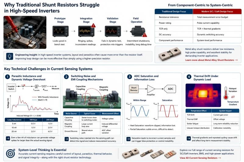
Instead of measuring a slowly changing current, today's current sensing circuits operate in an environment filled with fast switching edges, high electromagnetic fields, and rapidly changing current loops. Under these conditions, the resistor itself is rarely the weakest link. The surrounding electrical environment becomes equally important.
This explains why a resistor that performs perfectly in laboratory DC testing may produce unstable measurements once it is installed inside a high-power inverter.
| Traditional Design Focus | Modern SiC / GaN Design Focus |
|---|---|
| Resistance tolerance | Total measurement error budget |
| Power rating | Pulse current capability |
| TCR only | TCR + thermal gradients |
| DC accuracy | Dynamic switching accuracy |
| Component performance | System-level performance |
In practice, measurement degradation usually follows a predictable pattern.
Prototype stage: Current measurements appear clean during bench testing because switching current and bus voltage are still relatively low.
Integration stage: Once the inverter is connected to the motor and operated under full switching conditions, engineers begin to observe waveform ringing, unexpected current spikes, or inconsistent ADC readings.
Validation stage: The hardware passes static calibration but fails dynamic testing. Overcurrent protection occasionally triggers without any actual fault, or current measurements drift during long-duration operation.
Field operation: Customers report intermittent inverter shutdowns or unstable torque output. Engineers spend weeks debugging firmware before discovering that the real problem originates from PCB layout or sensing loop inductance rather than the resistor itself.
For high-current inverter platforms, many designers evaluate metal alloy shunt resistors because they provide low resistance, high pulse-current capability, and stable performance under demanding operating conditions. Even so, proper PCB layout and Kelvin routing remain essential to achieve the expected measurement accuracy.
One of the most common mistakes is replacing the resistor with a higher precision model while leaving the PCB layout unchanged. In many projects, improving loop geometry reduces measurement error far more effectively than reducing resistor tolerance from 1% to 0.1%.
Key Technical Challenges in Current Sensing Systems
Measurement errors in high-speed inverter systems rarely originate from a single source. Instead, they result from the interaction of several physical effects that occur simultaneously.
Individually, each effect may contribute only a small amount of error. Together, however, they can overwhelm the original sensing signal and significantly reduce system reliability.
Parasitic Inductance and Dynamic Voltage Overshoot
Parasitic inductance is often the largest hidden error source in high-speed current sensing.
Every conductor carrying current possesses inductance. This includes resistor terminals, PCB traces, copper planes, busbars, solder joints, and even the current probe used during debugging.
Although these inductances are usually measured in nanohenries, they generate substantial voltage when subjected to rapid current transitions.
| Loop Inductance | 100 A/μs | 200 A/μs |
|---|---|---|
| 5 nH | 0.5 V | 1.0 V |
| 10 nH | 1.0 V | 2.0 V |
| 20 nH | 2.0 V | 4.0 V |
Compare those voltages with a typical shunt output of only 50–100 mV, and the challenge becomes obvious. The transient voltage generated by parasitic inductance can exceed the useful measurement signal by an order of magnitude.
At that point, improving resistor tolerance has almost no effect because the dominant error source no longer comes from the resistor itself.
If your inverter switches above 100 A/μs, always estimate total loop inductance before selecting the resistor package. In many cases, layout dominates measurement accuracy.
Switching Noise and EMI Coupling Mechanisms
Fast switching edges behave like broadband electromagnetic transmitters. Every transition injects energy into nearby conductors through capacitive coupling, magnetic coupling, and shared impedance.
Unlike random electrical noise, switching interference is synchronized with inverter operation, making it extremely difficult to distinguish from legitimate current information.
| Noise Source | Typical Cause | Measurement Effect |
|---|---|---|
| Capacitive coupling | Sense traces close to switching nodes | Voltage spikes |
| Magnetic coupling | Large current loop area | Induced differential voltage |
| Ground bounce | Shared return path | ADC offset variation |
These errors rarely appear during schematic review. They emerge only after the PCB layout, power stage, and gate driver begin operating together.
ADC Saturation and Information Loss
The analog front-end has a limited input range. Once transient voltage exceeds this range, the converter cannot accurately reproduce the waveform.
There are two typical failure modes.
Hard saturation occurs when the amplifier output reaches its voltage limit. The resulting waveform becomes clipped, permanently removing information from that sampling instant.
Partial saturation is more difficult to detect. Only part of the transient is captured, causing subtle measurement errors that may be interpreted as genuine current variation.
In EV motor drives, these corrupted samples often appear during acceleration, regenerative braking, or sudden torque changes—exactly when current measurement accuracy is most important.
Thermal Drift Under Dynamic Load
Thermal behavior in SiC and GaN systems differs significantly from traditional DC applications.
Instead of experiencing constant heating, the resistor is repeatedly exposed to varying pulse currents, changing switching frequencies, and localized heating near power terminals.
Different temperatures across the resistor body, solder joints, and copper pads may generate thermal electromotive force (Thermal EMF), while repeated expansion and contraction accelerate mechanical fatigue.
Applications requiring extremely stable resistance over a wide temperature range often evaluate metal foil current detection resistors, especially where long-term measurement stability and low drift are critical.
| Temperature Effect | System Impact |
|---|---|
| TCR Drift | Current gain error |
| Thermal EMF | Offset voltage |
| Solder fatigue | Long-term reliability reduction |
| Uneven hotspot distribution | Calibration instability |
Engineers selecting current sensing resistors for high-frequency inverter systems should therefore evaluate electrical performance, thermal stability, pulse capability, and PCB implementation as a complete measurement solution rather than considering the resistor alone.
Conclusion
SiC and GaN technologies have fundamentally changed the way engineers approach current measurement. In high-speed inverter systems, achieving reliable current sensing is no longer determined by resistor tolerance alone. PCB layout, parasitic inductance, Kelvin connection, thermal behavior, and signal conditioning all contribute to the final measurement accuracy.
Selecting the right current sensing resistor therefore requires evaluating the entire measurement chain rather than comparing datasheet specifications in isolation. A properly matched resistor, combined with optimized PCB routing and robust thermal design, helps improve control stability, protection accuracy, and long-term system reliability in EV traction inverters, industrial motor drives, energy storage systems, and other high-power applications.
If your project requires a custom resistance value, specialized package, low-inductance structure, or application-specific engineering support, working with an experienced manufacturer can significantly shorten development time and reduce design risk.
Prosemi provides a wide range of low-ohm current sensing solutions, including metal alloy current sense resistors, metal alloy shunt resistors, slim sampling resistors, and metal foil current detection resistors for demanding power electronics applications.
For technical consultation, custom design requests, or product recommendations based on your application requirements, please contact our engineering team. We will help you select the most suitable current sensing solution for your inverter, BMS, or high-power conversion system.