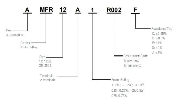
AMFR12
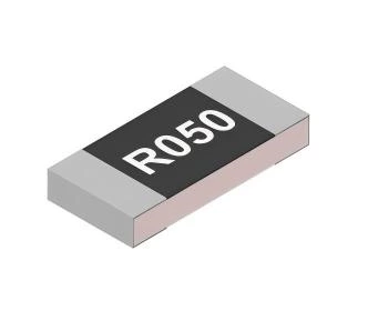
Low-Resistance Metal Film Chip Resistor
Applications
- Consumer electronics
- Computer & relative products
- Communication devices
- Measuring instrument
- Industrial / Power supply
- Battery management system
-
AEC-Q200 qualified Current Sensing Resistor
Features
- Low Resistance / TCR / Inductance(≦5NH)
- Excellent long-term stability
- High precision current sensing
- High power capability
- Halogen free and lead free
- RoHS compliant
- AEC-Q200 compliant
Part Numbering System
| Type | Rating Power at 70℃ |
T.C.R. (ppm/℃) |
Resistance Range(mΩ) | Meterial | Operating Temperature(℃) |
|
| C:0.25% | D:0.5%,F:1.0%, G:2.0%,J:5.0% |
|||||
| AMFR12 | 0.25W,0.75W 0.5W,1W |
±150 | - | 39mΩ≤R<50mΩ | Metal Alloy | -55~+155℃ |
| ±100 | - | 50mΩ≤R<100mΩ | ||||
| ±50 | 470mΩ≤R≤10Ω | 100mQ≤R≤10Ω | ||||
| AMFR25 | 1W,2W 3W |
±50 | 470mΩ≤R≤10Ω | 100mΩ≤R≤10Ω | ||
| Type | Rating Power at 70℃ |
T.C.R. (ppm/℃) |
Resistance Range(mΩ) F:1.0%,G:2.0%,J:5.0% |
Meterial | Operating Temperature(℃) |
|---|---|---|---|---|---|
| AMFR12 | 0.25W 0.5W |
±200 | 10mΩ≤R<39mΩ | Metal Alloy | -55~+155℃ |
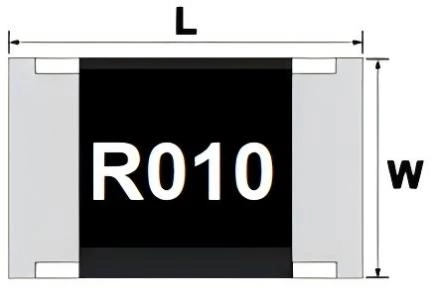
Construction
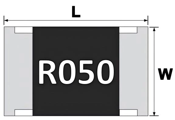
Unit: mm
| Type | L | W | H | l₁ | l₂ |
|---|---|---|---|---|---|
| AMFR12 | 3.1±0.1 | 1.6±0.1 | 0.55±0.1 | 0.4±0.2 | 0.45±0.2 |
| AMFR25 | 6.3±0.2 | 3.2±0.2 | 0.55±0.1 | 0.65±0.25 | 0.65±0.25 |
| AMFR25 3W |
0.7±0.15 |
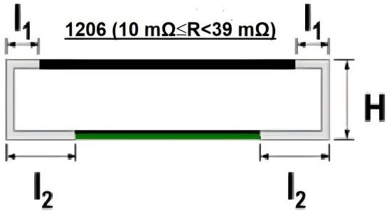
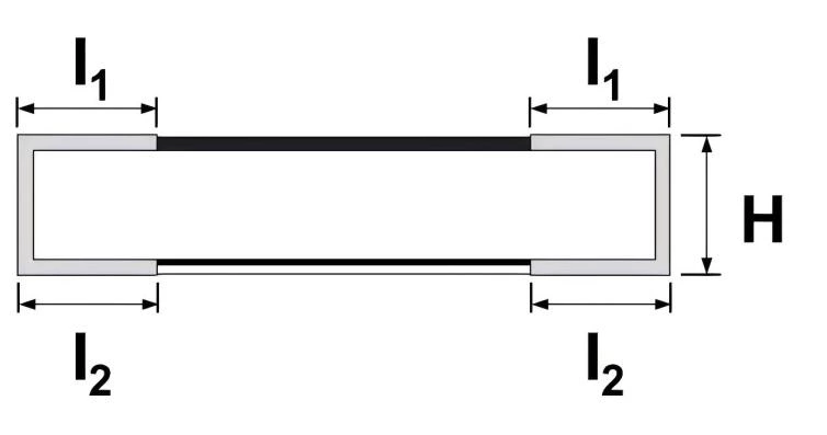
Unit: mm
| Type | L | W | H | I₁ | l₂ |
|---|---|---|---|---|---|
| AMFR12 (10mΩ≤R<39mΩ) |
3.3±0.2 | 1.7±0.2 | 0.65±0.2 | 0.2±0.15 | 0.68±0.2 |
Recommended land pattern
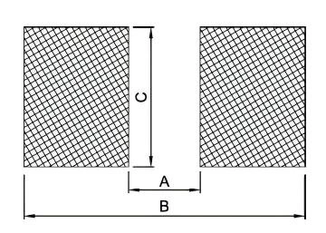
Unit: mm
| Type | A | B | C |
|---|---|---|---|
| AMFR12 | 2.2 | 4.2 | 1.8 |
| AMFR12 (10mΩ≤R<39mΩ) |
1.2 | 4.8 | 1.84 |
| AMFR25 | 4.9 | 8.1 | 3.4 |
Product Characteristics
| Item | Test condition/Methods | Limited |
|---|---|---|
| Temperature coefficient of resistance |
TCR=(R-R0)/R0(T2-T1)X 10⁶ R0:resistance of room temperature R:resistance of 125℃ T1:Room temperature T2:Temperature at 125℃ |
Refer to Spec |
| Short time Overload | Standard power:6.25 times rated power whichever is less for 5 seconds. |
±(1.0%+0.001Ω) |
| High power (2X/4X)and wide terminal type:5 times rated power whichever is less for 5 seconds. |
||
| Resistance to Soldering Heat |
260±5℃ for 10 seconds. | ±(1.0%+0.001Ω) No Visual damage |
| Temperature Cycling | -55℃ to+155℃,300 cycles | ±(1.0%+0.001Ω) No Visual damage |
| High Temperature Exposure |
At 155±5℃ for 1000 hours. | ±(1.0%+0.001Ω2) |
| Bias Humidity | 1,000 hours;85℃/85%RH,10%of operating power.Measurement at 24±4 hours after test conclusion. |
±(0.5%+0.05Ω) |
| Leaching | 260±5℃ for 30 seconds. | >95%Coverage No Visual damage |
| Insulation Resistance | Apply 100VDC for 1 minute. | ≥10GΩ |
| Damp Heat with Load |
40±2℃,90~95%R.H.RCWW or Max.working current whichever is less for 1000 hrs with 1.5 hrs "ON"and 0.5 hr “OFF” |
±(1.0%+0.001Ω) |
| Solderability | 245±5℃ for 3 seconds. | >95%Coverage No Visual damage |
| Load Life (Endurance) |
70±2℃,Rated power,or Max.working current whichever is less for 1000 hrs with 1.5 hrs "ON" and 0.5 hr "OFF". |
±(0.5%+0.05Ω) |
| Resistance to Solvent |
The tested resistor be immersed into isopropyl alcohol of 20~25℃ for 60 secs. Then the resistor is left in the room for 48 hrs |
±(1.0%+0.001Ω) No Visual damage |
| Bending Strength | Bending once for 5 seconds D:1206=3mm 2512=2mm |
±(1.0%+0.001Ω) No Visual damage |
Construction
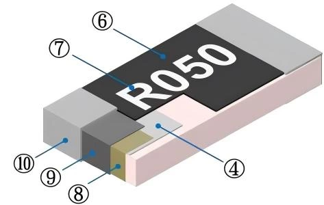
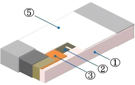
| ① | Alumina Substrate | ⑥ | Top Protective Overcoat |
| ② | Resistive Layer | ⑦ | Marking |
| ③ | Bottom Inner Electrode(Cu) | ⑧ | Side Inner Electrode |
| ④ | Top Inner Electrode | ⑨ | Barrier Layer(Ni) |
| ⑤ | Bottom Protective Overcoat White(≥39mR) Green(<39mR) |
⑩ | Solder coating (Sn) |
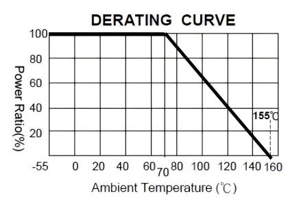
Power Derating Curve
The Operating Temperature Range: -55°C ~+155°C.
Power rating or current rating is in the case based on continuous full-load at ambient temperature of 70°C. For operation at ambient temperature in excess of 70°C, the load should be derated in accordance with figure of derating Curve.
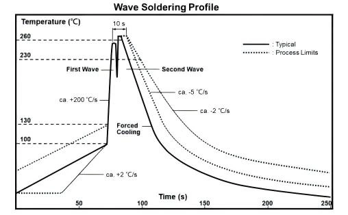
Wave solder Temperature condition
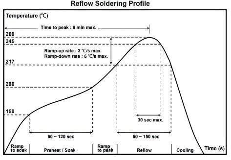
Solder reflow Temperature condition
Rework temperature(hot air equipment):350℃, 3~5seconds
Recommended reflow methods
IR, vapor phase oven, hot air oven
If reflow temperatures exceed the recommended profile, devices may not meet the
performance requirements.
Tapping & Package

Unit: mm
| Type | A ±0.2 |
B ±0.2 |
W +0.2 |
E ±0.05 |
F ±0.05 |
G ±0.1 |
H ±0.05 |
T ±0.1 |
D | P ±0.1 |
|---|---|---|---|---|---|---|---|---|---|---|
| 1206 | 1.9 | 3.05 | 8.0 | 1.75 | 3.5 | 4.0 | 2.0 | 0.75 | 1.50+0.1/-0 | 4.0 |
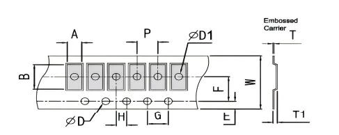
Unit: mm
| Type | A ±0.2 |
B ±0.2 |
W +0.1 |
E ±0.1 |
F ±0.05 |
G ±0.1 |
H ±0.05 |
T ±0.1 |
D | D1 ±0.1 |
T1 ±0.15 |
P ±0.1 |
|---|---|---|---|---|---|---|---|---|---|---|---|---|
| 2512 | 3.4 | 6.7 | 12.0 | 1.75 | 5.5 | 4.0 | 2.0 | 0.23 | 1.50+0.1/-0 | 1.5 | 0.85 | 4.0 |
Reel Specification
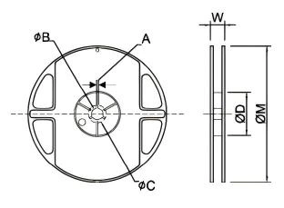
Unit: mm
| Type | Quantity (pcs) |
A | B | C | D | W | M |
|---|---|---|---|---|---|---|---|
| 1206 | 5,000 | 2.0±0.5 | 13.5±1 | 21±1 | 60±1 | 11.5±2 | 178±2 |
| 2512 | 4,000 | 16.0±2 |
Storage Data:
Storage time at the environment temp: 25±5℃& humidity: 60±20% is valid for one year from the date of delivery.