How to Design Multi-Stage Protection (Fuse + TVS + ESD)
Multi-stage protection combines complementary devices so each stage handles the threats it’s best at: a fuse handles sustained overcurrent, a TVS handles high-energy surges and transients, and dedicated ESD suppressors protect sensitive high-speed I/O from very fast electrostatic discharges. A well-designed chain maximizes reliability while minimizing size, cost, and nuisance trips.
1. Protection philosophy — why multi-stage?
Redundancy of function + specialization: each device type solves different problems (slow/large energy vs fast/low energy vs ESD).
Energy partitioning: the fuse or series element limits energy; the TVS absorbs bulk surge energy; ESD diodes clamp sub-ns pulses at the connector.
Prevent single-point failure: one device alone can be overloaded or too slow; stages protect downstream components and each other.
2. Typical stages and roles
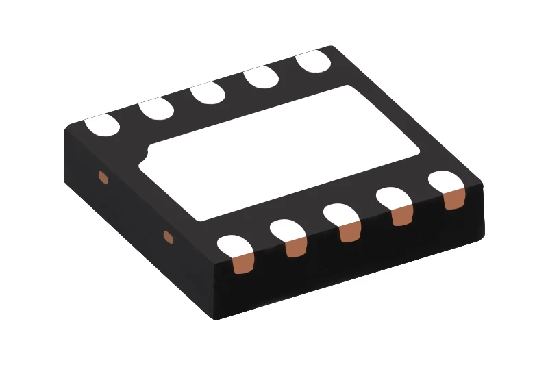
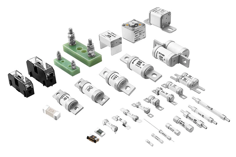
(1)Primary overcurrent protection (Fuse / PPTC / SMD fuse)
- Stops sustained overcurrent and faults.
- Must handle expected continuous current and clear short circuits safely.
(2)Surge protection (TVS diode / transient suppressor)
- Clamps high-energy transients (lightning-induced surges, inductive switching, load dump in automotive).
- Selected for standoff voltage, clamping voltage, peak pulse power, and surge waveform compatibility.
(3)Fast ESD protection (ESD diodes / arrays / GDT for high voltage)
- Protects data lines and connectors from IEC 61000-4-2 contact/air discharges.
- Very low capacitance variants required for high-speed interfaces.
(4)Optional intermediate elements
- Series resistor / ferrite bead / common-mode choke for damping and limiting inrush, improving TVS survivability.
- RC snubbers for repetitive switching transients.
3. Selection guidelines — how to choose each stage
(1)Fuse
-
Type: SMD chip fuse for PCB, blade or bolt fuse for harnesses, PPTC for resettable consumer circuits (only if appropriate).
-
Rated current: slightly above maximum expected continuous current (consider derating for ambient temp).
-
Blow characteristic: fast-blow for sensitive circuits; slow-blow for inrush-prone loads.
-
Breaking capacity: must be ≥ worst-case short-circuit current available from the source.
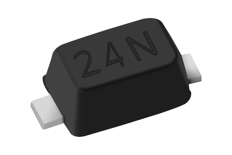
(2)TVS diode
-
Working (standoff) voltage (Vw): just above maximum operating voltage.
-
Clamping voltage (Vc): low enough to protect downstream electronics but above any allowable transient.
-
Peak pulse power (PPP) and energy rating: must handle the surge (e.g., 10/1000 µs automotive, 8/20 µs lightning-like).
-
Package & junction capacitance: for power lines, capacitance is less critical; for signal lines, choose low-capacitance TVS.
(3)ESD suppressor (for signal/data lines)
-
IEC 61000-4-2 rating: ensure device can handle contact/air discharge levels you target (±8 kV, ±15 kV etc.).
-
Low capacitance for high-speed lines (≤ 1–2 pF typical for USB 2.0/3.x, HDMI).
-
Array vs single channel: arrays reduce board area for multi-lane connectors.
(4)Series elements (resistor, bead, choke)
-
Resistor: limits fault current into TVS, but causes voltage drop—use small value if needed.
-
Ferrite bead / choke: reduces di/dt into TVS and filters HF noise; select impedance at target frequency.
4. PCB layout & placement rules (practical tips)
Order of placement: connector → ESD diodes (closest) → TVS (near connector but behind ESD) → series element/fuse → circuit.
Shortest path to ground for clamps: keep TVS/ESD cathode return traces as short and wide as possible to minimize inductance.
Avoid long traces between TVS and protected IC; long inductive traces raise clamping voltage.
Thermal relief for fuses: ensure adequate copper for heat dissipation and reliable solder joints.
Keep sensitive nets away from high-energy components: physical separation between power-surge path and signal return loops.
Place series beads/resistors close to the TVS to limit current into the clamp.
Use solid ground plane for low impedance return; stitch with vias near clamp pads.
Silkscreen/polarity: mark TVS polarity and fuse orientation for assembly inspection.
5. Test strategy (what to test and why)
Functional tests: normal operation, inrush current, thermal performance at max ambient.
Short-circuit test: verify fuse clears and downstream survives (or is isolated).
Surge tests: apply representative surge waveforms (e.g., 1.2/50 µs or 8/20 µs) to verify TVS clamping and energy handling.
ESD tests: IEC 61000-4-2 contact/air discharge on connector pins; confirm no data corruption or latch-up.
Automotive-specific: ISO 7637 pulses, load dump tests, and temperature/vibration qualification (if applicable).
Repeated stress & life tests: multiple surge pulses to validate long term survivability.
Note: use a lab-rated surge/ESD generator or accredited test lab for standardized testing.
6. Common mistakes & how to avoid them
Placing TVS too far from connector → raises clamp voltage; keep it close.
Insufficient fuse breaking capacity → fuse may not clear or may explode; verify source short-circuit capability.
Using PPTC where single-use fuse is required (e.g., safety-critical or high-energy applications) → PPTC may not isolate sufficiently.
Ignoring PCB inductance → inductance in traces increases transient voltage seen by ICs.
Using high-capacitance suppressors on high-speed lines → causes signal integrity issues.
Poor thermal design around fuse/TVS → shortens life or causes nuisance trips.
7. Practical example designs
Example A — USB-A / USB-C Port Protection (5 V data+power)
-
Connector → low-capacitance ESD array (closest to plug, protect D+/D−/SS pairs) → series common-mode choke for USB data (if needed) → TVS array (low Vw ~6 V for 5 V bus, low capacitance for data lanes) → polyfuse or SMD fuse on VBUS (rated slightly above 1–3 A depending on port) → buck regulator / downstream circuitry.
-
Notes: Use TVS with low clamping for VBUS, but ensure clamping still above USB device tolerant levels. Keep ESD clamps within <1 mm of connector if possible.
Example B — Automotive 12 V Input for ECU
-
Battery/ignition line → input blade fuse / high-breaking SMD fuse → series common choke / inrush limiting resistor → TVS designed for automotive load dump (standoff ~24–36 V or per system nominal) → transient suppression network / surge arrester → DC-DC converter.
-
Add transient voltage suppressors rated for ISO 7637 and TVS modules with high PPP (10/1000 µs energy capability). Use varistors or GDTs where needed for extreme surges.
8. Component selection checklist (quick reference)
Fuse: type, rated current, I²t, breaking capacity, package
TVS: standoff voltage, clamping voltage, PPP (pulse power), capacitance, package thermal dissipation
ESD: IEC 61000-4-2 rating, capacitance, leakage current, packaging (SOT-23, array)
Series bead/resistor: impedance at switching frequencies, DC resistance, power rating
Layout: trace width, ground vias near clamps, spacing for creepage/clearance
9. BOM example (illustrative, not vendor-specific)
SMD fuse 2 A fast-blow, 1206, I²t / breaking capacity per design
TVS power diode 600 W (peak pulse), Vw ≈ 14 V (for 12 V systems)
Low-capacitance TVS array for USB data lanes (≤ 1.5 pF)
ESD diode array for connector pins, ±15 kV IEC 61000-4-2 rating
Ferrite bead 0805, Z at 100 MHz = 600 Ω for EMI suppression
10. Final checklist before release
Validate fuse sizing vs continuous and inrush currents (and ambient derating)
Confirm TVS standoff and clamping meet device max voltage plus margin
Ensure ESD diodes have acceptable capacitance for data lines
Check PCB placement: clamps near connector, short returns to ground plane
Run standardized ESD and surge tests; iterate layout if clamping voltage too high
Document failure modes and serviceability (replaceable fuse? access?)
Review regulatory/safety requirements for your product domain (automotive, medical, consumer)
Conclusion
Designing multi-stage protection is about matching device strengths to threat characteristics and paying strict attention to layout. Fuse + TVS + ESD is a proven pattern: the fuse isolates sustained faults, the TVS absorbs large energy transients, and ESD diodes protect against fast, localized charges on connectors and signal lines. Good component selection, short PCB return paths, and standardized testing are the keys to a robust solution.