From Selection To Commissioning: Master Entire Process Of High-power Current Shunt Resistors
In inverters, motor drives and industrial high-power power supplies, shunt resistors not only have to withstand constant current impacts of tens or even hundreds of amperes, but also maintain measurement stability for a long time. To achieve neither excessive heat generation nor provide precise current feedback, it is necessary to strive for excellence in every aspect, including selection, heat dissipation, PCB layout and calibration. This article will guide you to start from the characteristics of the device, break down the core design points, and combine real cases to help you master the application secrets of high-power current-sensing resistors throughout the process.
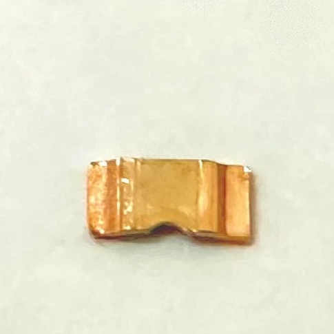
Fundamentals of Current Shunt Resistor
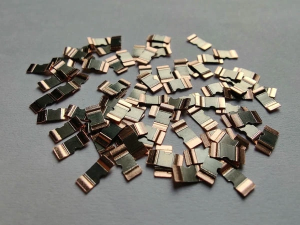
1.1 How Shunt Resistors Work
A current shunt resistor converts a large current into a small, proportional voltage drop according to Ohm’s law. That millivolt-level signal is then amplified by a differential amplifier for shunt resistors and digitized by an ADC.
1.2 Key Specifications
-
Resistance Value (≤5 mΩ): Balances sensitivity (higher mΩ) against power dissipation (lower mΩ).
-
Power Rating (100 W–500 W+): Ensures safe operation under continuous high currents.
-
Temperature Coefficient (≤50 ppm/°C): Guarantees stability across –40 °C to +85 °C.
-
Tolerance (±0.5%–1%): Defines initial accuracy before calibration.
2. Selecting the Right Shunt Resistor
2.1 Define Your Application Requirements
-
Power Supplies & Inverters: Choose through-hole high-power shunt resistors rated ≥200 W for robust thermal handling.
-
Electric Vehicles: Opt for surface-mount shunts (100 W SMD, 1–5 mΩ) to minimize size and weight.
-
Smart-Grid Monitoring: Prioritize ultra-low drift and high stability in industrial-grade shunt sensors.
2.2 Sizing Resistance and Power
Determine Resistance Value:
- For maximum resolution → 2 mΩ–5 mΩ
- For minimal insertion loss → ≤1 mΩ
Apply Power Margin: Multiply expected current²×R by 1.2–1.5 to select a resistor with sufficient power headroom.
Evaluate Thermal Path: Ensure your choice supports adequate heat sinking or airflow.
3. PCB Layout & Thermal Management Best Practices
3.1 Kelvin (Four-Wire) Connections
-
Separate current-carrying traces from voltage-sense leads to eliminate parasitic trace resistance.
-
Run sense traces as short as possible, directly into your differential amplifier’s input.
3.2 High-Current Trace Design
-
Use wide copper pours or multiple parallel traces.
-
Add thermal vias beneath and around the shunt to spread heat into inner layers.
3.3 Heat-Dissipation Strategies
-
Mount resistors on the top layer with direct airflow.
-
Consider external heatsinks or forced-air cooling for continuous high-power operation.
4. Commissioning: Installation, Calibration & Testing
4.1 Pre-Installation Checks
-
Verify part numbers, resistance values, and power ratings against BOM.
-
Inspect solder joints and ensure Kelvin pins are accessible.
4.2 Functional Calibration
-
Zero-Current Offset: Record the amplifier’s output with no current; adjust zero-offset in firmware.
-
Full-Scale Calibration: Pass a known reference current; calculate actual vs. expected voltage drop and apply gain correction.
-
Linearity Verification: Test at multiple current points (25%, 50%, 75%, 100%) to confirm linear response.
4.3 Thermal and Environmental Validation
-
Perform a temperature drift test from –40 °C to +85 °C, ensuring final error stays within tolerance.
-
Conduct long-duration stress tests at rated current to check for thermal runaway or drift over time.
5. FAQ (Common Questions & Solutions)
Q1: Why use four-wire Kelvin connections?
They isolate sensing leads from current-carrying paths, removing measurement errors from PCB trace resistance.
Q2: How can I reduce power loss in my shunt resistor?
Choose a lower resistance value, improve heat sinking, and maximize amplifier gain to minimize insertion loss.
Q3: What power margin should I leave?
A 20%–50% safety margin (i.e., choose a resistor rated 1.2×–1.5× your maximum expected dissipation) extends lifetime and prevents overheating.
Q4: How do I guard against electrical noise?
Use RC filtering on the sense inputs, maintain a clean ground plane, and keep sense leads as short as possible.
Conclusion
From precise high-power shunt resistor selection to meticulous PCB layout, robust thermal management, and rigorous on-site commissioning, every step is vital to achieving high accuracy and long-term reliability. By following these guidelines—defining application requirements, applying Kelvin wiring, calibrating systematically, and validating under real-world conditions—you’ll master the entire process and unlock the full potential of high-power current measurement in your industrial, automotive, or smart-grid projects.